
DDR4 SO‑DIMM
JEDEC-standard DDR4 small-outline memory module for platforms using a 260‑pin SO‑DIMM architecture. Published configurations cover 2666 and 3200 MHz at capacities up to 32 GB.
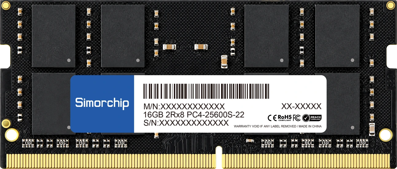
Technical Summary
Key Features
- JEDEC-standard module design
- Edge connector gold plating, 10 µin minimum
- SPD programmed and verified in production
- IQC, IPQC, FQC and OQC production quality control
- RoHS / REACH / CE / FCC compliant
- Limited Lifetime Warranty
Ordering Information
SIMORCHIP industrial ordering part numbers are listed below. Contact SIMORCHIP for configurations not listed.
Industrial Ordering Part Numbers
| Ordering P/N | Capacity | Data rate | CL | Rank | Component composition | Voltage | Datasheet |
|---|---|---|---|---|---|---|---|
| SMC04G8S4E32 | 4 GB | 3200 MHz | CL22 | 1Rx8 | 512M x 8, 8C | 1.2 V | On Request → |
| SMC08G8S4E26 | 8 GB | 2666 MHz | CL19 | 1Rx8 | 1024M x 8, 8C | 1.2 V | On Request → |
| SMC08G8S4E32 | 8 GB | 3200 MHz | CL22 | 1Rx8 | 1024M x 8, 8C | 1.2 V | On Request → |
| SMC08GFS4E32 | 8 GB | 3200 MHz | CL22 | 2Rx8 | 512M x 8, 16C | 1.2 V | On Request → |
| SMC16G8S4E32 | 16 GB | 3200 MHz | CL22 | 1Rx8 | 2048M x 8, 8C | 1.2 V | On Request → |
| SMC16GFS4E26 | 16 GB | 2666 MHz | CL19 | 2Rx8 | 1024M x 8, 16C | 1.2 V | On Request → |
| SMC16GFS4E32 | 16 GB | 3200 MHz | CL22 | 2Rx8 | 1024M x 8, 16C | 1.2 V | On Request → |
| SMC32GFS4E32 | 32 GB | 3200 MHz | CL22 | 2Rx8 | 2048M x 8, 16C | 1.2 V | On Request → |
Each ordering part number has its own datasheet, available on request. Capacity, rank and component composition are stated per part number rather than per family.
Electrical & Timing Specifications
Mechanical Specifications
Environmental Specifications & Compliance
Operating temperature is specified as DRAM case temperature (TC).
Compatibility & Qualification
Check the DIMM socket, memory controller, board layout and firmware when selecting a module. Compatibility is verified on the target configuration according to the project requirements.
Industrial Program Controls
Production Verification
Production-level verification
- Incoming, in-process, final and outgoing quality control
- SPD programming and verification
- Module functional verification before shipment
Project-level qualification
- Target-platform compatibility verification
- Stability verification under the defined operating conditions
- Application-specific qualification where the program requires it
Production-level verification is part of the manufacturing flow. Project-level qualification is scoped per program.
Technical Documentation
Product Configuration Review
Provide the target platform architecture, required capacity, data rate, operating conditions and expected program lifecycle. SIMORCHIP engineering will review the applicable module configuration and qualification requirements.